
The P-N junction diode is appeared in
the year 1950. It is the most essential and the basic building block of
the electronic device. The PN junction diode is a two terminal device,
which is formed when one side of the PN junction diode is made with
p-type and doped with the N-type material. The PN-junction is the root
for semiconductor diodes. The various electronic components like BJTs, JFETs, MOSFETs (metal–oxide–semiconductor FET), LEDs and analog or digital ICs
all supports semiconductor technology. The main function of the
semiconductor diode is, it facilitates the electrons to flow totally in
one direction across it. Finally, it acts as a rectifier. This article
gives a brief information about the PN junction diode, PN junction diode
in forward bias and reverse bias and the VI characteristics of PN
junction diode
What is a PN Junction Diode?
There are three possible biasing conditions and two operating regions for the typical PN-Junction Diode, they are: zero bias, forward bias and reverse bias.
When no voltage is applied across the PN
junction diode then the electrons will diffuse to P-side and holes will
diffuse to N-side through the junction and they combine with each
other. Therefore, the acceptor atom close to the P-type and donor atom
near to the N-side are left unutilized. An electronic field is generated
by these charge carriers. This opposes further diffusion of charge
carriers. Thus, no movement of the region is known as depletion region
or space charge.

PN Junction Diode
If we apply forward bias to the
PN-junction diode, that means negative terminal is connected to the
P-type material and the positive terminal is connected to the N-type
material across the diode which has the effect of decreasing the width
of the PN junction diode.
If we apply reverse bias to the
PN-junction diode, that means positive terminal is connected to the
P-type material and the negative terminal is connected to the N-type
material across the diode which has the effect of increasing the width
of the PN junction diode and no charge can flow across the junction

VI Characteristics of PN Junction Diode
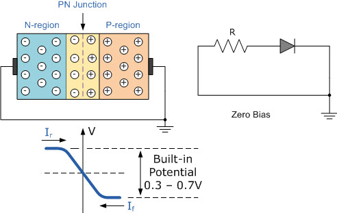
Zero Biased PN Junction Diode
In the zero bias junction, potential
provides higher potential energy to the holes on the P and N side
terminals. When the terminals of the junction diode are shorted, few
majority charge carriers in the P-side with plenty energy to overcome
the potential barrier to travel across the depletion region. Therefore,
with the help of majority charge carriers, the current starts to flow in
the diode and it is denoted to as forward current. In the same way,
minority charge carriers in the N-side move across the depletion region
in reverse direction and it is referred to as reverse current.
Zero Biased PN Junction Diode
Potential barrier opposes the movement
of electrons & holes across the junction and permits the minority
charge carriers to drift across the PN junction. However, the potential
barrier helps minority charge carriers in P-type and N-type to drift
across the PN-junction, then an equilibrium will be established when the
majority charge carriers are equal and both moving in reverse
directions, so that the net result is zero current flowing in the
circuit. This junction is said to be in a state of dynamic equilibrium.
When the temperature of the
semiconductor is increased, minority charge carriers have been endlessly
generated and thus leakage current starts to rise. But, electric
current cannot flow since no external source has been connected to the
PN-junction.
PN Junction Diode in Forward Bias
When a PN-junction diode is connected in a forward bias
by giving a negative voltage to the N-type and a positive voltage to
the P-type material. If the external voltage becomes more than the value
of the potential barrier (estimate 0.7 V for Si and 0.3V for Ge, the
opposition of the potential barriers will be overcome and the flow of
current will start.Because, the negative voltage repels electrons near
to the junction by giving them the energy to combine and cross over with
the holes being pushed in the opposite direction to the junction by the
positive voltage.
PN Junction Diode in Forward Bias
The result of this in a characteristic
curve of zero current flowing up to built in potential is called as
“knee current” on the static curves & then a high current flow
through the diode with a slight increase in the external voltage as
shown below.
VI Characteristics of PN Junction Diode in Forward Bias
The VI characteristics of PN junction
diode in forward bias are non linear, that is, not a straight line. This
nonlinear characteristic illustrates that during the operation of the N
junction, the resistance is not constant. The slope of the PN junction
diode in forward bias shows the resistance is very low. When forward
bias is applied to the diode then it causes a low impedance path and
permits to conduct a large amount of current which is known as infinite
current. This current starts to flow above the knee point with a small
amount of external potential.

PN Junction Diode VI Characteristics in Forward Bias
The potential difference across the PN
junction is maintained constant by the depletion layer action. The max
amount of current to be conducted is kept incomplete by the load
resistor, because when the PN junction diode conducts more current than
the normal specifications of the diode, the extra current results in the
heat dissipation and also leads to serve damage to the device.
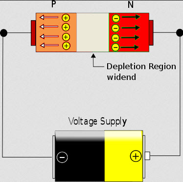
PN Junction Diode in Reverse Bias
When a PN junction diode is connected in
a Reverse Bias condition, a positive (+ Ve) voltage is connected to the
N type material & a negative (-Ve) voltage is connected to the
P-type material.
When the +Ve voltage is applied to the
N-type material, then it attracts the electrons near the positive
electrode and goes away from the junction, whereas the holes in the
P-type end are also attracted away from the junction near the negative
electrode.
PN Junction Diode in Reverse Bias
In this type of biasing, current flow
through the PN junction diode is zero. Though, the current leakage due
to minority charge carriers flows in the diode that can be measured in a
uA (micro amperes). As the potential of the reverse bias to the PN
junction diode ultimately increases and leads to PN junction reverse
voltage breakdown and the current of the PN junction diode is controlled
by an external circuit. Reverse breakdown depends on the doping levels
of the P & N regions. Further, with the increase in reverse bias the
diode will become short circuited due to overheat in the circuit and
max circuit current flows in the PN junction diode.
VI Characteristics of PN Junction Diode in Reverse Bias
In this type of biasing, the
characteristic curve of diode is shown in the fourth quadrant of the
below figure. The current in this biasing is low till breakdown is
reached and hence the diode looks like as open circuit. When the input
voltage of the reverse bias has reached the breakdown voltage, reverse
current increases enormously.

PN Junction Diode VI Characteristics in Reverse Bias
Therefore, this is all about PN junction
diode in zero bias, forward bias and reverse bias conditions and VI
characteristics of PN junction diode.We hope that you have got a better
understanding of this concept.Furthermore, any doubts regarding this
article, or electronics projects
please give your feedback by commenting in the comment section
below.Here is a question for you, which diode is used in the photo
transistor ?
Photo Credits:
- PN Junction Diode by ustudy
- VI characteristics of PN junction diodeby tutorvista
- Zero Biased PN Junction Diode by expertsmind


Best ias coaching in bangalore
ReplyDelete.www.globalias.in
ReplyDeleteBest ias coaching in bangalore
.www.globalias.in